MOSFET Integrated Circuit
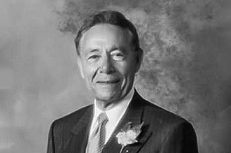
Mohamed Mohamed Atalla (Arabic: محمد محمد عطاالله; August 4, 1924 – December 30, 2009) was an Egyptian–American engineer, physical chemist, cryptographer, inventor and entrepreneur. He was a semiconductor pioneer who made important contributions to modern electronics.
His invention of the MOSFET (metal–oxide–semiconductor field-effect transistor, or MOS transistor) in 1959, along with his earlier surface passivation and thermal oxidation processes, revolutionized the electronics industry. He is also known as the founder of the data security company Atalla Corporation (now Utimaco Atalla), founded in 1972. He received the Stuart Ballantine Medal (now the Benjamin Franklin Medal in physics) and was inducted into the National Inventors Hall of Fame for his important contributions to semiconductor technology as well as data security.
Born in Port Said, Egypt, he was educated at Cairo University in Egypt and then Purdue University in the United States, before joining Bell Labs in 1949 and later adopting the more anglicized "John" or "Martin" M. Atalla as professional names. He made several important contributions to semiconductor technology at Bell, including his development of the surface passivation and thermal oxidation processes (the basis for silicon semiconductor technology such as the planar process and monolithic integrated circuit chips), his invention of the MOSFET (with Dawon Kahng) in 1959, and the PMOS and NMOS fabrication processes.
Atalla's pioneering work at Bell contributed to modern electronics, the silicon revolution, and Digital Revolution. The MOSFET in particular is the basic building block of modern electronics, and is considered one of the most important inventions in electronics. It is also the most widely manufactured device in history, and the US Patent and Trademark Office calls it a "groundbreaking invention that transformed life and culture around the world".
His invention of the MOSFET was initially overlooked at Bell, which led to him resigning from Bell and joining Hewlett-Packard (HP), founding its Semiconductor Lab in 1962 and then HP Labs in 1966, before leaving to join Fairchild Semiconductor, founding its Microwave & Optoelectronics division in 1969. His work at HP and Fairchild included research on Schottky diode, gallium arsenide (GaAs), gallium arsenide phosphide (GaAsP), indium arsenide (InAs) and light-emitting diode (LED) technologies.
He later left the semiconductor industry, and became an entrepreneur in cryptography and data security. In 1972, he founded Atalla Corporation, and filed a patent for a remote Personal Identification Number (PIN) security system. In 1973, he released the first hardware security module, the "Atalla Box" which encrypted PIN and ATM messages, and went on to secure the majority of the world's ATM transactions.
He later founded the Internet security company TriStrata Security in the 1990s. In recognition of his work on the PIN system of information security management as well as cybersecurity, Atalla has been referred to as the "Father of the PIN" and an information security pioneer. He died in Atherton, California, on December 30, 2009.
- 1Early life and education (1924–1949)
- 2Bell Telephone Laboratories (1949–1962)
- 3Hewlett-Packard (1962–1969)
- 4Fairchild Semiconductor (1969–1972)
- 5Atalla Corporation (1972–1990)
- 6TriStrata Security (1993–1999)
- 7Later years and death (2000–2009)
- 8Awards and honors
- 9References
- 10External links
Early life and education (1924–1949)
Mohamed Mohamed Atalla[2][3][4] was born in Port Said, Egypt.[5] He studied at Cairo University in Egypt, where he received his Bachelor of Science degree. He later went to the United States, to study mechanical engineering at Purdue University. There, he received his master's degree (MSc) in 1947 and his doctorate (PhD) in 1949, both in mechanical engineering.[5] His MSc thesis was "High Speed Flow in Square Diffusers" published in 1948,[6] and his PhD thesis was "High Speed Compressible Flow in Square Diffusers" published in January 1949.[3]
Bell Telephone Laboratories (1949–1962)
After completing his PhD at Purdue University, Atalla was employed at Bell Telephone Laboratories (BTL) in 1949.[7] In 1950, he began working at Bell's New York City operations, where he worked on problems related to the reliability of electromechanical relays,[8] and worked on circuit-switched telephone networks.[9]
With the emergence of transistors, Atalla was moved to the Murray Hill lab, where he began leading a small transistor research team in 1956.[8] Despite coming from a mechanical engineering background and having no formal education in physical chemistry, he proved himself to be a quick learner in physical chemistry and semiconductor physics, eventually demonstrating a high level of skill in these fields.[10] He researched, among other things, the surface properties of silicon semiconductors and the use of silica as a protective layer of silicon semiconductor devices.[7] He eventually adopted the alias pseudonyms "Martin" M. Atalla or "John" M. Atalla for his professional career.[4]
Between 1956 and 1960, Atalla led a small team of several BTL researchers, including Eileen Tannenbaum, Edwin Joseph Scheibner and Dawon Kahng.[11] They were new recruits at BTL, like himself, with no senior researchers on the team. Their work was initially not taken seriously by senior management at BTL and its owner AT&T, due to the team consisting of new recruits, and due to the team leader Atalla himself coming from a mechanical engineering background, in contrast to the physicists, physical chemists and mathematicians who were taken more seriously, despite Atalla demonstrating advanced skills in physical chemistry and semiconductor physics.[10]
Despite working mostly on their own,[10] Atalla and his team made significant advances in semiconductor technology.[11] According to Fairchild Semiconductor engineer Chih-Tang Sah, the work of Atalla and his team during 1956–1960 was "the most important and significant technology advance" in silicon semiconductor technology,[11][12] including the history of transistors[13] and microelectronics.[14]
Surface passivation by thermal oxidation
Further information: Surface passivation and Thermal oxidation
See also: Planar process, p–n junction isolation, and Invention of the integrated circuit
An initial focus of Atalla's research was to solve the problem of silicon surface states. At the time, the electrical conductivity of semiconductor materials such as germanium and silicon were limited by unstable quantum surface states,[15] where electrons are trapped at the surface, due to dangling bonds that occur because unsaturated bonds are present at the surface.[16] This prevented electricity from reliably penetrating the surface to reach the semiconducting silicon layer.[7][17] Due to the surface state problem, germanium was the dominant semiconductor material of choice for transistors and other semiconductor devices in the early semiconductor industry, as germanium was capable of higher carrier mobility.[18][19]
He made a breakthrough with his development of the surface passivation process.[7] This is the process by which a semiconductor surface is rendered inert, and does not change semiconductor properties as a result of interaction with air or other materials in contact with the surface or edge of the crystal.[20] The surface passivation process was first developed by Atalla in the late 1950s.[7][21] He discovered that the formation of a thermally grown silicon dioxide (SiO2) layer greatly reduced the concentration of electronic states at the silicon surface,[21] and discovered the important quality of SiO2 films to preserve the electrical characteristics of p–n junctions and prevent these electrical characteristics from deteriorating by the gaseous ambient environment.[22]
He found that silicon oxide layers could be used to electrically stabilize silicon surfaces.[23] He developed the surface passivation process, a new method of semiconductor device fabrication that involves coating a silicon wafer with an insulating layer of silicon oxide so that electricity could reliably penetrate to the conducting silicon below. By growing a layer of silicon dioxide on top of a silicon wafer, Atalla was able to overcome the surface states that prevented electricity from reaching the semiconducting layer. His surface passivation method was a critical step that made possible the ubiquity of silicon integrated circuits, and later became critical to the semiconductor industry.[7][17] For the surface passivation process, he developed the method of thermal oxidation, which was a breakthrough in silicon semiconductor technology.[24]
The surface passivation process was a breakthrough in silicon semiconductor research,[16][21][19] as it enabled silicon to surpass the conductivity and performance of germanium, and was the breakthrough that led to silicon replacing germanium as the dominant semiconductor material.[19][15] The process also laid the foundations for the monolithic integrated circuit chip, as it was the first time that high-quality silicon dioxide insulator films could be grown thermally on the silicon surface to protect the underlying silicon p-n junction diodes and transistors.[22]
Before the development of integrated circuit chips, discrete diodes and transistors exhibited relatively high reverse-bias junction leakages and low breakdown voltage, caused by the large density of traps at the surface of single crystal silicon. Atalla's surface passivation process became the solution to this problem. He discovered that when a thin layer of silicon dioxide was grown on the surface of silicon where a p–n junction intercepts the surface, the leakage current of the junction was reduced by a factor from 10 to 100. This showed that the oxide reduces and stabilizes many of the interface and oxide traps. Oxide-passivation of silicon surfaces allowed diodes and transistors to be fabricated with significantly improved device characteristics, while the leakage path along the surface of the silicon was also effectively shut off.[14]
His surface oxidation method provided a semiconductor surface that was insensitive to the environment.[8] This became a fundamental p–n junction isolation capability necessary for planar technology and integrated circuit chips.[14]
Atalla first published his findings in BTL memos during 1957, before presenting his work at an Electrochemical Society meeting in 1958,[25][26] the Radio Engineers' Semiconductor Device Research Conference.[8] The semiconductor industry saw the potential significance of Atalla's surface oxidation method, with RCA calling it a "milestone in the surface field."[8] The same year, he made further refinements to the process with his colleagues Eileen Tannenbaum and Edwin Joseph Scheibner, before they published their results in May 1959.[12][27]
According to Fairchild Semiconductor engineer Chih-Tang Sah, the surface passivation process developed by Atalla and his team "blazed the trail" that led to the development of the silicon integrated circuit.[14][12] Atalla's silicon transistor passivation technique by thermal oxide[28] was the basis for several important inventions in 1959: the MOSFET (MOS transistor) by Atalla and Dawon Kahng at Bell Labs, the planar process by Jean Hoerni at Fairchild Semiconductor, and the monolithic integrated circuit chip by Robert Noyce at Fairchild in 1959.[26][14][29] By the mid-1960s, Atalla's process for oxidized silicon surfaces was used to fabricate virtually all integrated circuits and silicon devices.[30] In addition to silicon semiconductor technology, the surface passivation process is also critical tosolar cell[31] and carbon quantum dot technologies.[20]
MOSFET (MOS transistor)
Main article: MOSFET
See also: PMOS logic, NMOS logic, and CMOS

MOSFET was invented by Atalla with his colleague Dawon Kahng in 1959, based on Atalla's earlier surface passivation and thermal oxidation processes.
Building on his earlier pioneering research[32] on the surface passivation and thermal oxidation processes,[24] Atalla developed the metal–oxide–semiconductor (MOS) process.[7] Atalla then proposed that a field effect transistor–a concept first envisioned in the 1920s and confirmed experimentally in the 1940s, but not achieved as a practical device—be built of metal-oxide-silicon. Atalla assigned the task of assisting him to Dawon Kahng, a Korean scientist who had recently joined his group.[7] That led to the invention of the MOSFET (metal–oxide–semiconductor field-effect transistor) by Atalla and Kahng,[33][34] in November 1959.[8] Attalla and Kahng first demonstrated the MOSFET in early 1960.[35][36] With its high scalability,[37] and much lower power consumption and higher density than bipolar junction transistors,[38] the MOSFET made it possible to build high-density integrated circuit (IC) chips.[39]
There were originally two types of MOSFET logic, PMOS (p-type MOS) and NMOS (n-type MOS).[33] Both types were developed by Atalla and Kahng when they originally invented the MOSFET. They fabricated both PMOS and NMOS devices with a 20 µm process. However, only the PMOS devices were practical working devices at the time.[34]
Atalla proposed the concept of the MOS integrated circuit chip in 1960. He noted that the MOS transistor's ease of fabrication made it useful for IC chips.[10] However, Bell Labs initially ignored MOS technology, as the company was not interested in ICs at the time.[10] Despite this, the MOSFET generated significant interest at RCA and Fairchild Semiconductor. Inspired by the first MOSFET demonstration by Atalla and Kahng in early 1960, researchers at RCA and Fairchild fabricated MOSFETs later that year, with Karl Zaininger and Charles Meuller fabricating a MOSFET at RCA, and Chih-Tang Sah building an MOS-controlled tetrode at Fairchild.[33]
His concept of the MOS IC chip eventually became reality,[10] starting with an experimental MOS chip demonstrated by Fred Heiman and Steven Hofstein at RCA in 1962, after which MOS would become thedominant fabrication process for IC chips.[40] CMOS, which combined aspects of both PMOS and NMOS, was later developed by Chih-Tang Sah and Frank Wanlass at Fairchild in 1963.[41] The development of MOS technology, which was capable of increasing miniaturisation, eventually became the focus of RCA, Fairchild, Intel and other semiconductor companies in the 1960s,fuelling the technological and economic growth of the earlysemiconductor industry in California (centred around what later became known as Silicon Valley)[42]as well as Japan.[43]
The MOSFET was the first truly compact transistor that could be miniaturised and mass-produced for a wide range of uses,[10] and went on to revolutionize the electronics industry.[44][45] The MOSFET forms the basis of modern electronics,[46] and is the basic element in most modern electronic equipment.[47] It is the most widely used semiconductor device in the world,[39][48] and the most widely manufactured device in history, with an estimated 13 sextillion MOS transistors manufactured as of 2018.[49][50]
The MOSFET is central to the microelectronics revolution,[51] silicon revolution,[15][52] and microcomputer revolution,[53] and is the fundamental building block of modern digital electronics during the Digital Revolution, information revolution and Information Age.[54][55][56][57]
It is used in a wide variety of electronics applications, such as computers, synthesizers,[17] communications technology, smartphones,[58] Internet infrastructure,[59][60][61] digital telecommunication systems,video games, pocket calculators, and digital wristwatches,among many other uses.[62]
It has been described as the "workhorse of the electronics industry" due to being the building block of every microprocessor, memory chip and telecommunication circuit in use.[63] TheUS Patent and Trademark Office calls the MOSFET a "groundbreaking invention that transformed life and culture around the world".[58] The invention of the MOSFET by Atalla and Kahng has been credited as "the birth of modern electronics"[64] and is considered to be possibly the most important invention in electronics.[65]
Nanolayer Transistor...
See also: Nanoelectronics and History of nanotechnology...